AsteraLabs-Blue-Grey-Hz_cropped
  • Applications
  • Products
    • Product Overview

      Built in the cloud, for the cloud.

      • Buy and Sample
    • Aries PCIe®/CXL™ Smart DSP Retimers

      Industry-proven Smart Retimers for PCI Express® (PCIe) 4.0, PCIe 5.0, and Compute Express Link™ (CXL) systems

    • Taurus Ethernet Smart Cable Modules™

      Overcome reach, signal integrity, and bandwidth utilization issues for 100G/Lane Ethernet connectivity

    • Leo CXL Smart Memory Controllers

      CXL-attached memory expansion, pooling, and sharing for cloud servers

  • Cloud-Scale Interop Labs
    • Aries PCIe/CXL Smart DSP Retimers

      Learn how Astera Labs enables you to deploy PCIe and CXL systems with confidence.

    • Leo CXL Smart Memory Controllers

      Learn how Astera Labs enables you to deploy CXL-attached memory with confidence.

  • Technology Insights
    • Articles

      Browse our knowledge base articles for information about our products and technologies.

    • Video Center

      Explore our educational and technical video center to support your design needs.

    • Document Library

      Find app notes, white papers and more in our technical resource library.

    • FAQs

      Find answers to the most frequently asked questions about our products and technologies.

    • Webinars

      Created by engineers for engineers, our webinar series explores the most important topics related to hyperscale datacenters.

  • Careers
  • About
    • About Us
    • Executive Team
    • Support Portal    
    • Quality
    • News & Articles
    • Events
  • Contact

PCIe 5.0

Home » PCIe » PCIe 5.0

PCI Express® 5.0 Architecture Channel Insertion Loss Budget

June 11, 2020 by AsteraAdmin

The upgrade from PCIe® 4.0 to PCIe 5.0 doubles the bandwidth from 16GT/s to 32GT/s but also suffers greater attenuation per unit distance, despite the PCIe 5.0 specification increasing the total insertion loss budget to 36dB. After deducting the loss budget for CPU package, AIC, and CEM connector, merely 16dB system board budget remains. Within the remaining budget, engineers need to consider safety margin for board loss variations due to temperature and humidity.

By Liang Liu, Systems and Applications Engineer, Astera Labs – PCI-SIG® Member

Written by Astera Labs for PCI-SIG

PCI Express® (PCIe®) technology is the most important high-speed serial bus in servers. Due to its high bandwidth and low latency characteristics, PCI Express architecture is widely used in various server interconnect scenarios, such as:

  1. Within a Server: CPU to GPU, CPU to Network Interface Card, CPU to Accelerator, CPU to SSD
  2. Within a Rack: CPU to JBOG and JBOF through board-to-board connector or cable
  3. Emerging GPUs-to-GPUs or Accelerators-to-Accelerators interconnects

At the same time, with the rapid development of heterogeneous computing, the data throughput requirements in the server system are becoming higher and higher. Two years after the release of the PCIe 4.0 specification, the PCIe 5.0 specification was officially released in May 2019. PCIe 5.0 technology still uses the same 128b / 130b coding scheme, and the symbol rate increased from 16 GT/s to 32 GT/s. In keeping with tradition, the PCIe 5.0 specification is backwards compatible with lower-speed PCIe generations.

The Challenge of PCIe 5.0 Technology Design

In the case of other standards greater than 30 GT/s, the PAM-4 modulation method is usually used to make the signal’s Nyquist frequency one-quarter of the data rate, at the cost of 9.5 dB signal-to-noise ratio (SNR). However, PCIe 5.0 architecture continues to use the non-return-to-zero (NRZ) signaling scheme, thus the Nyquist frequency of the signal is one-half of the data rate, which is 16 GHz. The higher the frequency, the greater the attenuation. The signal attenuation caused by the channel insertion loss (IL) is the biggest challenge of PCIe 5.0 technology system design.

PCIe 5.0 specification outlines the bump-to-bump IL budget as 36 dB for 32 GT/s, and the bit error rate (BER) must be less than 10-12. To address the problem of high attenuation to the signal, the PCIe 5.0 specification defines the reference receiver such that the continuous-time linear equalizer (CTLE) model includes an ADC (adjustable DC gain) as low as -15 dB, whereas the reference receiver for 16 GT/s is only -12 dB. The reference decision feedback equalizer (DFE) model includes three taps for 32 GT/s and only two taps for 16 GT/s.

In addition, the possibility of errors on the serial link becomes higher as the data rate reaches 32 GT/s. Due to the significant role of the DFE circuit plays in the receiver’s overall equalization, burst errors are more likely to occur compared to 16 GT/s. To counteract this risk, PCIe 5.0 architecture introduces precoding in the protocol. After enabling precoding at the transmitter side and decoding at the receiver side, the chance of burst errors is greatly reduced, thereby enhancing the robustness of the PCIe 5.0 specification 32 GT/s Link.

PCIe 5.0 Technology Channel Insertion Loss Budget

Table 1 uses a typical system base board plus add-in card (AIC) application as an example to list the insertion loss budget for PCIe 4.0 architecture (16GT/s) and PCIe 5.0 architecture (32 GT/s). At 32 GT/s, after deducting 9 dB for the CPU package, 9.5 dB for the AIC, and 1.5 dB for the CEM connector, the remainder for the system base board is only 16 dB.

Table 1: 16 GT/s and 32 GT/s Channel Insertion Loss Budget
PCIe® Rev Total Channel Insertion Loss Budget Root Package CEM Connector Add-in Card (AIC) Remaining Budget for System Base Board
3.0 (8 GT/s) 22 dB 3.5 dB 1.7 dB 6.5 dB 10.3 dB
4.0 (16 GT/s) 28 dB 5.0 dB 1.5 dB 8.0 dB 13.5 dB
5.0 (32 GT/s) 36 dB 9.0 dB 1.5 dB 9.5 dB 16.0 dB

However, when looking at the 16-dB system base board budget, engineers need to consider the following factors:

  1. As the PCB temperature rises, the IL of the PCB trace becomes higher
  2. Process fluctuation during PCB manufacturing can result in slightly narrower or wider line widths, which can lead to fluctuations in IL
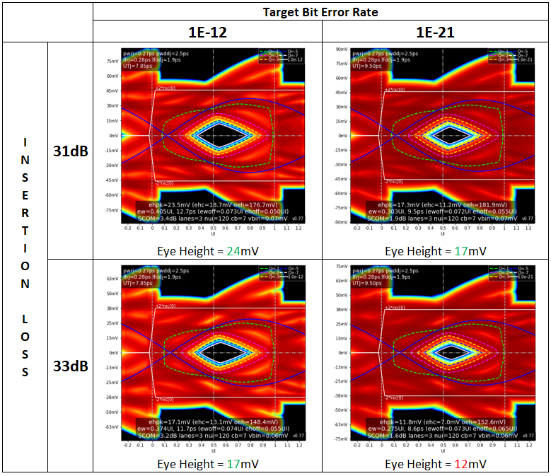
  3. The amplitude of the Nyquist frequency signal (16-GHz sine wave in the case of 32 GT/s NRZ signaling) at the source side is 800 mV pk-pk, which will reduce to about 12.7 mV after 36 dB of attenuation. This underscores the need to leave some IL margin for the receiver to account for reflections, crosstalk, and power supply noise that all potentially will degrade the SNR.
Figure 1: Insertion Loss Budget for System Base Board

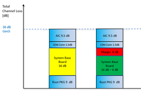
Thus, the IL budget reserved for the PCB trace on the system base board should be 16 dB minus some amount of margin which is reserved for the above factors. Many hardware engineers and system designers tend to leave 10-20% of the overall channel IL budget as margin for such factors. In the case of a 36-dB budget, this amounts to 4-7 dB.

As the demand for artificial intelligence and machine learning increases, PCIe 5.0 technology will enable more and more system topologies. The change from PCIe 4.0 architecture to PCIe 5.0 architecture brings the channel IL budget from 28 dB to 36 dB, which will bring new design challenges. By leveraging advanced PCB materials and/or PCIe 5.0 Retimers to ensure sufficient end-to-end design margin, system designers can ensure a smooth upgrade to PCIe 5.0 architecture.

Reference

  1. AN 835: PAM4 Signaling Fundamentals https://www.intel.com/content/dam/www/programmable/us/en/pdfs/literature/an/an835.pdf

Filed Under: Smart Retimers Tagged With: PCI-SIG, PCIe, PCIe 4.0, PCIe 5.0

Simulating with Retimers for PCIe® 5.0

March 16, 2020 by Casey Morrison

The design solution space for high-speed serial links is becoming increasingly complex as data rates climb, channel topologies become more diverse, and tuning parameters for active components multiply. PCI Express® (PCIe®) 5.0, at 32 GT/s, is a particularly relevant example of an application whose design solution space can be a daunting problem to tackle given the low-cost nature of its end-equipment. This paper is intended to help system designers navigate through these design challenges by providing a how-to guide for defining, executing, and analyzing system-level simulations including PCIe® 5.0 Root Complex (RC), Retimer, and End Point (EP).

Download Paper
Download Slides

Scope

The scope of this analysis includes:

  • PCIe 5.0 and Compute Express Link™ (CXL™) topologies up to 32 GT/s data rate
  • Low-cost/high-temperature-variation and high-cost/low-temperature-variation PCB materials
  • Root Complex (RC), protocol-aware Retimer, and End-Point (EP) devices
  • SeaSim and IBIS-AMI Simulation models and methodologies

The approach is based on IBIS Algorithmic Modeling Interface (IBIS-AMI) simulations. IBIS-AMI’s standardized interface offers interoperability between models provided by different integrated circuit (IC) vendors. More importantly, critical component-level impairments such as jitter, bandwidth, and equalization adaptation consistency can be represented in IBIS-AMI models and reflected in the overall link performance—effects that a simple s-parameter analysis of the passive interconnect fails to capture.

For the purposes of this paper, models of a worst-case PCIe transmitter and receiver are used for the RC and EP. A Retimer is used between the RC and EP to achieve a channel reach extension. Its placement is extensively studied, and the overall system performance is investigated using time-domain simulation with IBIS-AMI device models. The methodology outlined here can be extended to any RC, Retimer, and EP device; and it can be performed with any Channel Simulator.

In the context of PCI Express, a Retimer is a physical-layer-protocol-aware, software-transparent extension device that forms two separate electrical Link Segments: RC to Retimer, and Retimer to EP. In addition to clock and data recovery, a Retimer must participate in the Link equalization protocol whereby each transmitter—RC, Retimer, and EP—is automatically optimized for the benefit of the Link partner receiver. A block diagram of a typical Retimer is shown in Figure 1.

Figure 1: Retimer Block Diagram

Figure 1: Retimer Block Diagram

Approach

A how-to guide is presented to help system engineers approach the PCIe 5.0 and CXL system design challenge in a methodical and bounded manner.

The proposed steps include:

  1. Determine if a Retimer is required. Use the statistical eye analysis simulator (SeaSim) tool to determine if the topology meets the PCIe channel requirements, if it is marginal to those requirements and may benefit from a Retimer, or if it clearly does not meet the requirements and cannot operate without a Retimer. Consider the performance degradations associated with temperature, humidity, and manufacturing variations.
  2. Define a simulation space. Identify the worst-case conditions (e.g. temperature, humidity, and impedance) and the minimum set of parameters (e.g. transmitter Presets) which must be varied to adequately analyze system performance and margin.
  3. Define the evaluation criteria. Determine the minimum eye height and width which will be considered a passing result and the minimum set/number of transmitter settings which must yield a passing result to have high confidence that there is adequate margin.
  4. Execute the simulation matrix and analyze the results. Use IBIS-AMI models and time domain simulations to analyze each case in the context of the pre-defined evaluation criteria.

The purpose of this analysis is to be more instructional than theoretical, leaving the reader with a concrete set of steps that can be applied whenever they are faced with a similar design challenge involving RC, Retimer, EP, and PCB material co-optimization.

Step 1: Determine if a Retimer is Required

Before evaluating an RC + Retimer + EP Link, you must first understand whether a Retimer is required for the Link. There are typically two ways of reaching this conclusion:

  1. Compare the end-to-end channel insertion loss, including RC and EP package losses, against the PCIe channel budget (Table 1). If the topology’s channel loss exceeds the PCIe informative specification, then a Retimer is likely required.
  2. Simulate the channel s-parameter in the Statistical Eye Analysis Simulator (SeaSim) tool which implements a reference PCIe transmitter and PCIe receiver to determine if the post-equalized eye height (EH) and eye width (EW) meet the minimum eye opening requirements for the reference receiver: ≥15 mV EH and ≥0.3 UI EW at Bit Error Ratio (BER) ≤ 10-12. If the eye opening does not meet the reference receiver’s requirements, then a Retimer is likely required. This methodology is more accurate and preferred to the pure loss budget analysis, as it takes into account other channel characteristics, such as reflections and crosstalk, as well as reference PCIe device equalization capabilities.

In this analysis we consider a two-connector PCIe topology which is common in server, storage, and accelerator systems (Figure 2).

Figure 2: System Board + Riser Card + AIC Topology

Figure 2: System Board + Riser Card + AIC Topology

The topology includes various loss components for which PCIe has established a budget. Table 1 shows the breakdown of these loss components for PCIe 4.0 (reference) and PCIe 5.0 & CXL.

Table 1: Total Channel Insertion Loss Budget Breakdown

1. System Board budget includes the baseboard, riser card, the baseboard-to-riser-card, and PCIe card electromechanical (CEM) form factor connectors

Topology 1: No Retimer, Ultra-Low-Loss PCB Material

For such a topology, the main challenge at 32 GT/s is meeting the system board loss budget (16 dB at 16 GHz) for a 12-inch baseboard channel plus riser card. For the first topology analyzed in this paper, an ultra-low-loss PCB material such as Megtron-6 (~1 dB/inch at 16 GHz) is used for this topology to reduce the baseboard loss as much as possible, as shown in Figure 3.

Figure 3: Topology 1 using Ultra-Low-Loss PCB Material

Figure 3: Topology 1 using Ultra-Low-Loss PCB Material

Although such systems typically operate at nominal temperature (~25 C) and humidity (45-55%), it is important to examine the channel characteristics at extreme conditions such as high temperature (80 C), high humidity (>75%), and worst-case PCB trace manufacturing tolerance leading to differential pair impedance deviation (85 Ω + 10% = 93 Ω). Under these circumstances, the insertion loss degrades to ~1.11 dB/inch at 16 GHz. The channel s-parameters for this topology across different operating conditions are shown in Figure 4 below.

Figure 4: Topology 1 End-to-End Channel Insertion Loss for Nominal Conditions, Humid 80-C Environment , and 93-Ω Impedance and Humid 80-C Environment

Figure 4: Topology 1 End-to-End Channel Insertion Loss for Nominal Conditions, Humid 80-C Environment , and 93-Ω Impedance and Humid 80-C Environment

To further confirm that a Retimer is required for this topology to operate, SeaSim simulations, shown in Figure 5, are run for each scenario: (a) nominal temperature/humidity conditions (differential pair impedance 85 Ohm, temperature ~25 C and humidity 45-55%), (b) high temperature/humidity (differential pair impedance 85 Ohm, temperature ~80 C and humidity 75%), and (c) 93-Ω impedance with high temperature/humidity (differential pair impedance 93 Ohm, temperature ~80 C and humidity 75%).

Figure 5a: SeaSim Result for Nominal Conditions

Figure 5a: SeaSim Result for Nominal Conditions

Figure 5b: SeaSim Result for Humid 80-C Environment

Figure 5b: SeaSim Result for Humid 80-C Environment

Figure 5c: SeaSim Result for 93-Ω Impedance and Humid 80-C Environment

Figure 5c: SeaSim Result for 93-Ω Impedance and Humid 80-C Environment

IBIS-AMI channel simulations performed in bit-by-bit mode, which is analogous to time domain simulations, with a reference transmitter and reference receiver model also yields a post-equalized eye that does not meet the minimum eye dimensions of criterion 2. Figure 6 shows the testbench used for this simulation.

Figure 6: Keysight ADS Simulation Schematic for Topology 1

Figure 6: Keysight ADS Simulation Schematic for Topology 1

The transmitter IBIS-AMI model represents a reference transmitter with three-tap finite impulse response (FIR) filter as defined in the PCIe specification. Likewise, the receiver IBIS-AMI model represents a reference receiver with a four-pole/two-zero continuous time linear equalizer (CTLE) and a three-tap decision feedback equalizer (DFE) as defined in the PCIe specification.

Three sets of IBIS-AMI simulations are performed to further validate the initial finding that a Retimer is needed for this channel topology (refer to Figure 4 for insertion loss plots). The simulation results are summarized in Table 2.

1.a) Topology 1 assuming nominal temperature, nominal humidity, and 85-Ω impedance
1.b) Topology 1 assuming high temperature (80 C), high humidity, and 85-Ω impedance
1.c) Topology 1 assuming high temperature (80 C), high humidity, and 93-Ω impedance

Table 2: Results Summary for Topology 1
(Reference Receiver with 15-dB CTLE gain and adaptive CDR/DFE)
Table 2: Results Summary for Topology 1

Topology 2: Retimer on Riser Card, Ultra-Low-Loss PCB Material

Given that the channel in Topology 1 fails both channel evaluation criteria, a second topology is considered in which a Retimer is added on the Riser Card, as shown in Figure 7. Adding a Retimer segments the channel into two independent halves, making it much easier to meet the PCIe channel specifications on each half.

Figure 7: Topology 2 with Retimer on Riser Card using Ultra-Low-Loss PCB Material

Figure 7: Topology 2 with Retimer on Riser Card using Ultra-Low-Loss PCB Material

Taking into account additional Retimer breakout routing and considering the worst-case conditions—high temperature, high humidity, and 93-Ω impedance due to manufacturing tolerance—the insertion loss for the two channel segments in Topology 2 are shown in Figure 8.

Figure 8: Topology 2 End-to-End Channel Insertion Loss for RC-to-Retimer Segment and Retimer-to-EP Segment

Figure 8: Topology 2 End-to-End Channel Insertion Loss for RC-to-Retimer Segment and Retimer-to-EP Segment

With considerably lower insertion loss, the SeaSim analysis shows there is ample margin for both Link segments, as shown in Figure 9.

Figure 9a: SeaSim Result for RC-to-Retimer Segment

Figure 9a: SeaSim Result for RC-to-Retimer Segment

Figure 9a: SeaSim Result for Retimer-to-EP Segment

Figure 9b: SeaSim Result for Retimer-to-EP Segment

Topology 3: Retimer on Baseboard, Low-Cost PCB Material

Space permitting, instead of the Riser Card, a Retimer can also be placed on the Baseboard as it is shown in Figure 10. With such a Retimer placement, the margins for each channel segment are relatively large compared to the “without Retimer” case. At this point, system designers can consider using higher loss PCB material to reduce the cost of the system. A lower cost material such as Megtron-4 will have ~1.9 dB/inch at 16 GHz under worst-case conditions and result in a 40-50% cost reduction in the baseboard.

Figure 10: Topology 3 with Retimer on Baseboard using Low-Loss PCB Material

Figure 10: Topology 3 with Retimer on Baseboard using Low-Loss PCB Material

Considering the worst-case conditions, the insertion loss for the two channel segments in Topology 3 are shown in Figure 11.

Figure 11: Topology 3 End-to-End Channel Insertion Loss for RC-to-Retimer Segment and Retimer-to-EP Segment

Figure 11: Topology 3 End-to-End Channel Insertion Loss for RC-to-Retimer Segment and Retimer-to-EP Segment

Despite higher loss per inch on the baseboard with the lower cost PCB material, there is still a considerable margin for both Link segments, as shown in Figure 12.

Figure 12a: SeaSim Result for RC-to-Retimer Segment

Figure 12a: SeaSim Result for RC-to-Retimer Segment

Figure 12b: SeaSim Result for Retimer-to-EP Segment

Figure 12b: SeaSim Result for Retimer-to-EP Segment

Step 2: Define a Simulation Space

The high-level simulation parameters used in all IBIS-AMI simulations presented in this work are shown in Table 3.

Table 3: Summary of High-Level Simulation Parameters

To achieve meaningful results in a reasonable timeframe, a narrow simulation space is chosen, as shown in Table 4. The approach used for selecting the simulation space is covered in a prior work [3], and the basic idea is to test multiple transmitter Preset settings as a means of gauging how robust the Link performance is. If a channel can pass for multiple Preset settings, this is a good indicator of healthy margin compared to a case where only one Preset works.

Table 4: Simulation Space

Transmitter Presets are pre-defined combinations of pre-shoot (pre-cursor equalization) and de-emphasis (post-cursor equalization). Table 5 shows the list of Preset settings considered in this analysis. It is worth noting that the every PCIe transmitter may implement slightly different pre-shoot and de-emphasis values for the ten defined presets, however the PCIe standard does define tolerances for these values with which every PCIe transmitter must comply.

Table 5: Transmitter Preset Settings

Keysight Advanced Design System (ADS) is the tool used to execute the IBIS-AMI simulations, measure the extrapolated EH and EW, and plot the post-equalized eye opening. For Topologies 2 and 3, two separate testbenches—RC to Retimer and Retimer to EP—are used to simulate the two separate Link segments, as shown in Figure 13 and Figure 14 below.

Figure 13: Keysight ADS Simulation Schematic for Topologies 2 and 3, RC to Retimer

Figure 13: Keysight ADS Simulation Schematic for Topologies 2 and 3, RC to Retimer

Figure 14: Keysight ADS Simulation Schematic for Topologies 2 and 3, Retimer to EP

Figure 14: Keysight ADS Simulation Schematic for Topologies 2 and 3, Retimer to EP

Step 3: Define the Evaluation Criteria

This analysis uses similar pass/fail criteria to that which was used in a prior work [3]. The criteria consist of two rules:

  1. A link must meet the receiver’s eye height (EH) and eye width (EW) requirements
  2. A link must meet criterion 1 for at least half of Tx Preset settings (≥5 out of 10)

Criterion 1 establishes that the there is a viable set of settings which will result in the desired BER. The specific EH and EW required by the receiver is implementation-dependent. For example, the Astera Labs receiver model requirements for post-equalized EH and EW are shown in Table 6. Criterion 2 ensures that the link has adequate margin and is not overly-sensitive to the Tx Preset setting.

Table 6: Astera Labs Receiver Model EH and EW Requirements

Step 4: Execute the Simulation Matrix and Analyze the Results

Topology 2 is simulated using the parameters and Tx Preset values noted in Step 2. Note that the minimum eye height and eye width requirement is set by the receiver model. For the Astera Labs Receiver model, the requirements are listed in Table 6. For the reference receiver model, the requirements are set by the PCIe standard.

Table 7: Topology 2 Results
Table 8: Topology 3 Results

A detailed data display of the pre-equalized channel pulse response and post-equalized eye contour are shown in Figure 15 and Figure 16 for Topology 2 and Topology 3, respectively.

Figure 15: Detailed Data Display for Topology 2, Tx Preset 9

Figure 15: Detailed Data Display for Topology 2, Tx Preset 9

Figure 16: Detailed Data Display for Topology 3, Tx Preset 9

Figure 16: Detailed Data Display for Topology 3, Tx Preset 9

Conclusions

This analysis shows that a channel topology which is common to PCIe 5.0 and CXL-based, at 32GT/s, server designs—baseboard plus riser card plus add-in card—may exceed the PCIe channel specifications and also the capabilities of a generic transmitter/receiver pair. By segmenting this channel topology into two with the use of a protocol-aware Retimer, simulations demonstrate that a more rigorous pass/fail criterion—achieving adequate eye height and width across at least half of all transmitter preset settings—can be met.

In fact, this analysis shows there is enough margin to allow for less expensive PCB material to be used, potentially reducing the total cost of the system substantially while still achieving robust performance on both link segments. This methodology of (1) determining if a Retimer is required, (2) defining a simulation space, (3) defining the evaluation criteria, and (4) executing the simulation matrix can be applied to a wide varied of PCIe 5.0 and CXL applications to help assess system performance and cost tradeoffs.

References

[1] https://pcisig.com/
[2] https://www.computeexpresslink.org/
[3] Yongyao Li, et al, “End-to-End System-Level Simulations with Repeaters for PCIe Gen4: A How-To Guide”, DesignCon 2017

Author Biographies

Elene Chobanyan is a signal integrity engineer at Hybrid IT Compute Solutions at Hewlett Packard Enterprise (HPE). She is HPE's primary voting member at PCI-SIG Electrical workgroup, a representative at IPC D24D standard and an active contributor at Gen-Z PHY workgroup. Elene received the B.S. degree in physics and the M.S. degree in electrical and electronics engineering from Tbilisi State University, Tbilisi, Georgia, and PhD. Degree in electrical and computer engineering from Colorado State University, USA. Her current focus areas are high speed server interconnect architecture and design, PCB material characterization techniques, non-volatile and volatile memory subsystems.

Casey Morrison is the head of Product and Applications Engineering at Astera Labs and is responsible for defining, validating, and helping customers design-in Astera Labs’ semiconductor products and plug-and-play systems. With 12+ years of experience in high-speed interfaces for data center and wired/wireless communications systems, he has a passion for creating chips and systems which help to enable state-of-the-art compute and networking topologies.

Pegah Alavi is a Senior Applications Engineer at Keysight Technologies, where she focuses on Signal Integrity and High Speed Digital Systems and Applications. Prior to joining Keysight Technologies, Pegah worked on system level modeling of analog and mixed signal circuits in order to best predict the overall systems performance and accurately represent each component.

    Filed Under: Smart Retimers Tagged With: DesignCon, PCIe, PCIe 5.0, PCIe Retimers

    PCI Express® Retimers vs. Redrivers: An Eye-Popping Difference

    June 26, 2019 by Casey Morrison

    Retimers and redrivers have enabled longer physical channels in servers and storage systems since Peripheral Component Interface (PCI) Express (PCIe®) 3.0 was first introduced more than 10 years ago. Now that PCIe 4.0 solutions are established, PCIe 5.0 solutions are ramping, and the PCIe 6.0 specification was released in early 2022, how do these reach extension tools stack up in the face of new challenges in high-speed connectivity?

    Redriver vs Retimers

    Figure 1: Redriver block diagram [1]
    A redriver is a mostly analog reach extension device designed to boost the high-frequency portions of a signal to counteract the frequency-dependent attenuation caused by the interconnect: the central processing unit (CPU) package, system board, connectors and so on. A redriver’s data path typically includes a continuous time linear equalizer (CTLE), a wideband gain stage and a linear driver. In addition, redrivers often have input loss–of–signal threshold and output receiver (Rx) detection capability. Figure 1 illustrates a typical redriver block diagram.

    retimer-block
    Figure 2: Retimer block diagram [1]
    A retimer is a mixed signal analog/digital device that is protocol-aware and has the ability to fully recover the data, extract the embedded clock and retransmit a fresh copy of the data using a clean clock. In addition to the CTLE and wideband gain stages also found in a redriver, retimers contain a clock and data recovery (CDR) circuit, a decision feedback equalizer (DFE) and a transmit (Tx) finite impulse response (FIR) driver. Finite state machines (FSMs) and/or a microcontroller typically manage the automatic adaptation of the CTLE, wideband gain, DFE and FIR driver, and implement the PCIe link training and status state machine (LTSSM).  Figure 2 illustrates a typical retimer block diagram.

    eye-attenuated
    Figure 3: Example of an eye attenuated by a channel (left), the eye after a redriver (middle) and the eye after a retimer (right)

    In simple terms, a redriver amplifies a signal, whereas a retimer retransmits a fresh copy of the signal. Figure 3 illustrates this and shows how an attenuated eye opening is boosted by a redriver and completely regenerated by a retimer.

    The PCIe 4.0 specification took the unprecedented step of formally defining the terms “retimer,” “redriver” and the superset term “repeater,” all of which are types of extension devices or components whose purpose is to extend the physical length of a link. The definitions are:

    • Repeater: An imprecise term for an extension device [2]. (This term causes confusion … please don’t use it!)
    • Redriver: A non-protocol-aware software-transparent extension device [2].
    • Retimer: A physical layer protocol-aware, software-transparent extension device that forms two separate electrical link segments [2].

    Use Cases for Retimers and Redrivers

    Reach extension devices are necessary whenever the channel – the electrical path between the root complex (RC) and endpoint (EP) – is longer than the PCIe specification allows. The specification defines the maximum channel length in terms of insertion loss at the Nyquist frequency (an informative specification, but easy to validate) and in terms of a reference receiver’s ability to sufficiently equalize and recover the data assuming a worst-case link partner transmitter (a normative specification, but time-consuming to validate). Suffice it to say, at PCIe 4.0 and beyond speeds, reach extension devices are necessary for:

    • Multiconnector topologies
    • Cabled topologies
    • Single-connector add-in card (AIC) topologies with baseboard channels longer than 9.5 inches

    Figure 4 shows an example of a two-connector “riser card” topology, which ordinarily would exceed the PCIe 4.0 loss budget of 28 dB. A redriver or retimer will enable reliable, error-free communication between the RC and EP. But how do you choose which one is the right tool for the job? Well, it helps to know more about the fundamental differences in their capabilities.

    redriver
    Figure 4: Example of redriver (top) and retimer (bottom) used in a two-connector topology

    Comparing Retimer and Redriver Capabilities

    Not all redrivers and retimers are the same. There are many distinctions between the two, which are universally true for all PCIe reach extension devices. For example:

    Retimers actively participate in the PCIe protocol; redrivers do not.

    The PCIe base specification spells out how and to what extent retimers participate in the protocol during Detect, Recovery, L0 and so on. Equalization to the L0 and L1 link states requires value-added functionality from the retimer (handshakes, timeouts, bit manipulation, etc.). Redrivers are unaware of and unparticipating in the protocol. If the link works reliably the first time, that’s great! But if the link experiences marginality of any sort, it becomes exceedingly difficult to pinpoint whether the problem is physically before the redriver or after it, since the redriver’s role in link formation is undefined and unknown to its link partners.

    Retimers reset the jitter and insertion loss budgets; redrivers do not.

    A retimer’s CDR fully recovers the data stream and retransmits it on a clean clock. Starting with a fresh copy of the data enables the extension of the channel to twice the original specification. Without a CDR, the best a redriver can do is attenuate (not reset) the data-dependent jitter (DDJ) caused by intersymbol interference (ISI). A redriver cannot attenuate uncorrelated or random jitter (RJ). In fact, a redriver will always add to RJ due to its own device thermal noise in a root-mean-square (RMS) manner [1].

    Retimers have a DFE; redrivers do not.

    A DFE compensates for reflections in the channel response caused by impedance discontinuities in board vias, connectors and package socket-board interfaces. The nice thing about a DFE is that it is unaffected by crosstalk. The DFE equalizes just as well in the presence of crosstalk, and once the data is sampled by the retimer’s CDR, crosstalk is eliminated for good. Redrivers use a CTLE that boosts both the signal and the noise [1]. Crosstalk is not eliminated or even attenuated through a redriver; in fact, it gets amplified.

    Retimers automatically adapt their receive and transmit equalizers to match the characteristics of the channel and the link partner’s needs; redrivers do not.

    A retimer will examine the signal it receives and adjust the CTLE and DFE to minimize its own bit error rate (BER). Likewise, the retimer’s transmitter will adjust its de-emphasis and pre-shoot equalization to minimize the link partner’s BER according to PCIe equalization protocol. A redriver, conversely, operates with a static equalizer setting. The optimal setting (which can be different for every channel in the system) is often painstakingly selected following an exhaustive search in Input/Output Buffer Information Specification (IBIS) algorithmic modeling interface (AMI) simulations and again in lab testing – a process fondly referred to as “tuning.”

    Retimers have built-in features to help diagnose link issues (both electrical and protocol); redrivers do not.

    Retimers have tools for assessing the electrical performance (internal eye monitors, pattern generators, pattern checkers) and protocol performance (link state history monitors, timeout adjustments). Redrivers cannot offer such diagnostic features because they are neither protocol-aware nor aware of the actual data passing through. Redrivers do not know what state the link is in.

    Retimers correct for lane-to-lane skew; redrivers do not.

    PCIe has a tight requirement on the physical skew between lanes on a board (1.6 ns for PCIe 4.0), typically caused by mismatches in channel routing length [3]. Retimers are required to compensate and reset any lane-to-lane skew, effectively doubling the specification budget. Redrivers cannot compensate for lane-to-lane skew, and what’s worse is that they may degrade the skew depending on how symmetric the redriver package is across all lanes.

    Retimers can be placed anywhere between two PCIe-compliant channels; redrivers cannot.

    By definition, retimers extend the total PCIe channel reach by two times the specification. A redriver’s reach extension, however, depends on where it is placed in the channel – how much loss is before the redriver versus how much is after [1]. The specific placement of a redriver must be carefully determined by IBIS-AMI simulation and experimentation. Too close to the root complex transmitter, and the redriver’s CTLE will enter nonlinear operation and will have limited benefit. Placed too far from the transmitter, the redriver’s device noise may significantly degrade the signal-to-noise ratio (SNR) of the data signal. It’s not all bad news for redrivers. They do have lower power consumption and lower input-to-output latency compared to retimers. But if the link does not form in the first place or if the BER is too high, none of that matters!

    Property

    Retimer

    Redriver

    PCIe Protocol Participation

    Protocol-aware

    Protocol-unaware

    Jitter Reduction

    Resets entire jitter budget (DDJ, RJ, etc.)

    Attenuates DDJ; amplifies RJ

    Equalization Capabilities

    CTLE, DFE, Tx FIR

    CTLE

    Adaptation

    CTLE, DFE and Tx FIR automatically adapt to the channel

    CTLE setting must be hand-selected based on simulation/experimentation

    Diagnostics Capabilities

    Receiver margining, eye diagram, eye width/height measurement, link state debugging information

    None to speak of

    Lane-to-Lane Skew Compensation Capabilities

    Resets entire skew budget

    Does not reset skew budget; may increase total skew

    Placement

    Anywhere with PCIe-compliant channels on the input and output sides

    Not too close to the source transmitter, but not far away either

    Usage in Closed Systems (i.e., systems where all endpoints are known and validated before release of the system) 

    Recommended; sanctioned use case in PCIe base specification

    Highly discouraged; use at your own risk after extensive simulation and testing [1]

    Usage in Open Systems (i.e., systems designed to be interoperable with any PCIe-compliant AIC) 

    Recommended; sanctioned use case in PCIe base specification

    Not recommended / discouraged [1]

    Table 1: Comparison of retimer and redriver capabilities and usage

    Outlook for PCIe Systems

    For PCIe 4.0/5.0 systems, all signs are pointing to an increased need for reach extension devices – and retimers in particular – due to several trends and challenges:

    • CPUs have more PCIe lanes per socket (>100 in some cases [4]) compared to PCIe 3.0. This leads to a greater number of PCIe slots and riser cards, denser routing, and an increased use of multiconnector topologies.
    • PCIe is shifting from an I/O bus to a multipurpose system interconnect. This means that more servers will be designed to be modular, allowing an array of compute, storage and networking resources to plug in to an increasing number of PCIe slots. This type of open, “plug anything in and it will work” server architecture requires a reach extension solution that is PCIe compliant with plug-and-play interoperability.
    • The disaggregation of resources such as modular servers, storage trays and accelerator trays is pushing endpoints physically away from CPUs, requiring cables or carrier cards to connect everything together. These longer physical topologies will increasingly need reach extension devices.
    • Systems are adopting a variety of interconnect styles – M.2, optical/copper link (OCuLink) cables and so on – all of which have unique lane-to-lane skew and crosstalk challenges that must be handled by the reach extension solution.
    • PCIe 5.0 technology is ramping quickly and there is pent-up demand across the industry for higher bandwidth. System designers are looking for a reach extension solution that can easily and quickly scale from 4.0 to 5.0 to 6.0 and beyond.

    In the end, system designers benefit from having multiple options for reach extension solutions. The exact performance requirements, physical constraints and cost targets for a server or storage system will guide the decision-making process, and the industry will benefit from knowing the trade-offs between retimer and redriver devices.

    Citations

    [1] Samaan, S., Froelich, D., and Johnson, S. (2015). High-Speed Serial Bus Repeater Primer: Re-driver and Re-timer Micro-Architecture, Properties, and Usage [White paper]. https://www.intel.com/content/dam/www/public/us/en/documents/white-papers/serial-bus-white-paper.pdf

    [2] PCI Express Base Specification Revision 5.0 Version 0.9, 2019. https://pcisig.com/

    [3] PCI Express Card Electromechanical Specification Revision 4.0 Version 0.9, 2019. https://pcisig.com/

    [4] Why AMD EPYC Rome 2P Will Have 128-160 PCIe Gen4 Lanes and a Bonus. https://www.servethehome.com/why-amd-epyc-rome-2p-will-have-128-160-pcie-gen4-lanes-and-a-bonus/

    Filed Under: Smart Retimers Tagged With: PCIe, PCIe 4.0, PCIe 5.0, PCIe Redrivers, PCIe Retimers

    The Impact of Bit Errors in PCI Express® Links: The Painful Realities of Low-Probability Events

    June 26, 2019 by Pulkit Khandelwal

    Peripheral Component Interconnect Express (PCIe®) 5.0 ushers in the era of >1 terabits per second (Tbps) of data bandwidth. Such immense bandwidth would be typical of a 16-lane (x16) link between two PCIe nodes, each lane operating at 32 Gbps.

    Given that the PCIe base specification mandates that a bit error ratio (BER) on each transceiver lane must be 1E-12 or better – that is, less than one error every 1E12, or 1 terabit – a bit-flip error could happen within the link every 1 s! Even a PCIe 4.0 link, if designed for the same BER specification, would have a bit-flip error every 2 s.

    Such bit errors are classified under the “correctable errors” category according to the PCIe specification. They do affect performance vis-à-vis latency and bandwidth, but no data/information is lost, and the PCIe fabric remains reliable. To get a better sense of the impact of errors, you need to consider the location of an error in the data stream and the time at which the error occurs in terms of the state of the PCIe Link Training and Status State Machine (LTSSM).

    In the L0 LTSSM state where data packets are transmitted and received, an erroneous bit received within Data Link Layer Packets (DLLPs) would lead to a failure in the data integrity check performed using the cyclic redundancy check (CRC) included with each transmitted packet. One of the salient features of PCIe is to ensure robust transmission. When the Data Link Layer detects an errored packet, it sends a negative acknowledgement (NACK) to its link partner. Upon receiving the NACK, the link partner restarts transmission from that packet onward. If the BER is within the specification, the only cost is a small hit to the link throughput and a momentary impact on latency (which can be shown to be greater than three times the normal latency with some basic math).

    Let’s now consider a more unforgiving example. PCIe uses a 128b/130b encoding scheme for 8.0-Gbps and higher rates. In this encoding scheme, each 130-bit block consists of a 2-bit sync header and a 128-bit data payload. There are two valid sync header encodings: 10b for data blocks and 01b for ordered set (non-data) blocks. Since these sync header bits occur every two bits within 130 bits, a simple probability analysis would reveal that, assuming all lanes are operating around the worst-case 1E-12 BER, there is a chance of an error happening on the sync header on some lane within a x16 link approximately once every minute.

    Having received an invalid sync header in the L0 link state, the PCIe controller, per the PCIe base specification, is expected to suspend data traffic and take the link to the Recovery LTSSM state. Upon entering the Recovery state, the PCIe controller allows the physical layer (PHY) transceivers to retrain, reacquire block lock and so on, thus getting an opportunity to re-establish optimal link health. The specification allows up to 1 µs for a trip through the Recovery LTSSM state. Needless to say, this adds a huge delay to the original errored packet – and all subsequent packets – until the link goes back to the L0 state.

    Besides sync headers, there are other protocol-related overhead tokens and data sets which, if corrupted, can also lead the link into the Recovery state. Table 1 shows the approximate probabilities of various data types being in error and the consequences of those errors.

    Relative-probabilities
    Table 1: Relative probabilities and consequences of different error events

    At this point, it’s worth noting that PCIe 5.0 introduces selectable “precoding,” which breaks an error burst into two errors: an entry error and an exit error. While this helps manage a burst of errors (caused by error propagation in a PHY receiver), it basically comes at a cost of turning a random single-bit error into two errors, thereby doubling the net BER and the aforementioned error probabilities.

    Tallying up all of the above, it is conceivable that a x16 PCIe 5.0 link would enter the Recovery LTSSM state approximately every 10 s, and it would replay a transaction layer packet (TLP) approximately every 1 s.

    Such frequent unplanned entries to the Recovery state (every 10 s) and TLP replays (every 1 s) will cause system health monitors in the baseboard management controller (BMC) to raise an alarm, and contribute to “latency tails,” which can have a considerable performance impact at the application layer [1].

    So what can you do to extract the full potential of a PCIe 5.0 link and avoid annoying, hard-to-diagnose “glitches” in the higher application layers? Well, one of the obvious solutions would be to design a system board with lower transmission (or insertion) loss in the channel. Using the SeaSim simulation tool from the PCI Special Interest Group (SIG) [2], Figure 1 shows eye diagrams from two channels: one with 31 dB of insertion loss and another with a higher 33-dB insertion loss. The simulations have two different BER targets: 1E-12, according to the specification; and 1E-21, which is akin to saying no errors at all. To ensure these BERs, the simulated eye height must meet or exceed 15 mV.

    Eye-diagram
    Figure 1: Eye diagram simulations using SeaSim

    You can see from these simulations that while the 33-dB loss channel would “pass” for a bit error target of 1E-12, it would not pass at 1E-21. The 31-dB loss channel does pass at 1E-21, however, with an eye height equivalent to the 33-dB channel at 1E-12. So in this very distinct analysis, backing off the insertion loss by 2 dB or so would imply going from the link entering the Recovery state every 10 s to almost never doing so at all.

    Upgrading printed circuit board (PCB) material to reduce transmission loss is a viable option to gain 2 dB of insertion loss, but may add a considerable expense, depending on board size. Alternatively, enhancements to PHY-layer transceiver circuitry to boost performance come at the cost of silicon power, area and complexity. And then there are certain system topologies that may turn out be marginal even when combining best-in-class transceiver technology and PCB materials, so aiming to achieve lower BERs on these topologies may be next to impossible. In such scenarios, you could take a divide-and-conquer approach by employing a PHY protocol-aware extension device, referred to in the PCIe specifications as a retimer. A retimer would split a stringent channel into separate smaller electrical link segments, each of which can operate with enough margin to achieve drastically lower BERs.

    While fairly limited at PCIe 3.0, such considerations became more widespread with current PCIe 4.0 deployments and will only grow with PCIe 5.0, as the signal integrity challenges far outpace the doubling of data rates.

    PCIe 5.0 systems are likely to see noticeably greater occurrences of link errors and TLP retries than current-generation systems. Thus, you must take care when setting a BER target for a PCIe link within a system. System designers typically account for device and environmental variations and set aside some electrical performance margin to safely keep a link operating at a BER mandated by the base specification. You must also factor in application-layer considerations given the nature of future data-center workloads, however. It would be prudent to target lower BERs for PCIe 5.0 and beyond.

    Citations

    1. Deierling, Kevin. “In Modern Datacenters, The Latency Tail Wags The Network Dog.” Nextplatform.com, March 27, 2018.

    2. PCI SIG Seasim Software Package

    Filed Under: Smart Retimers Tagged With: PCIe, PCIe 5.0, Signal Integrity

    Search

    Categories

    • Cloud-Scale Interop
    • Corporate
    • CXL Memory Connectivity
    • General
    • Smart Cable Modules
    • Smart Retimers

    Archives

    • October 2023
    • August 2023
    • June 2023
    • May 2023
    • March 2023
    • February 2023
    • January 2023
    • September 2022
    • August 2022
    • November 2021
    • October 2021
    • August 2021
    • December 2020
    • June 2020
    • March 2020
    • October 2019
    • June 2019
    • Aries PCIe/CXL Smart DSP Retimers
    • Taurus Ethernet Smart Cable Modules
    • Leo CXL Smart Memory Controllers
    • Cloud-Scale Interop Lab
    • Applications
    • Technology Insights
    • Contact Us
    • Careers
    • News & Articles
    • Support Portal    
    Subscribe for Updates
    Please enter your name.
    Please enter a valid email address.
    Subscribe

    Thanks for subscribing! 

    Something went wrong. Please check your entries and try again.

    By submitting this form, you are consenting to receive emails from Astera Labs. You can revoke your consent at any time by using the Unsubscribe link found at the bottom of every email.

    AsteraLabs-WhitewBug-Hz
    𝕏

    Copyright © 2023 Astera Labs, Inc. All rights reserved.

    Site Map I Privacy Policy I Terms of Use | Terms of Sale | Terms of Purchase | Code of Conduct