The design solution space for high-speed serial links is becoming increasingly complex as data rates climb, channel topologies become more diverse, and tuning parameters for active components multiply. PCI Express® (PCIe®) 5.0, at 32 GT/s, is a particularly relevant example of an application whose design solution space can be a daunting problem to tackle given the low-cost nature of its end-equipment. This paper is intended to help system designers navigate through these design challenges by providing a how-to guide for defining, executing, and analyzing system-level simulations including PCIe® 5.0 Root Complex (RC), Retimer, and End Point (EP).
Scope
The scope of this analysis includes:
- PCIe 5.0 and Compute Express Link™ (CXL™) topologies up to 32 GT/s data rate
- Low-cost/high-temperature-variation and high-cost/low-temperature-variation PCB materials
- Root Complex (RC), protocol-aware Retimer, and End-Point (EP) devices
- SeaSim and IBIS-AMI Simulation models and methodologies
The approach is based on IBIS Algorithmic Modeling Interface (IBIS-AMI) simulations. IBIS-AMI’s standardized interface offers interoperability between models provided by different integrated circuit (IC) vendors. More importantly, critical component-level impairments such as jitter, bandwidth, and equalization adaptation consistency can be represented in IBIS-AMI models and reflected in the overall link performance—effects that a simple s-parameter analysis of the passive interconnect fails to capture.
For the purposes of this paper, models of a worst-case PCIe transmitter and receiver are used for the RC and EP. A Retimer is used between the RC and EP to achieve a channel reach extension. Its placement is extensively studied, and the overall system performance is investigated using time-domain simulation with IBIS-AMI device models. The methodology outlined here can be extended to any RC, Retimer, and EP device; and it can be performed with any Channel Simulator.
In the context of PCI Express, a Retimer is a physical-layer-protocol-aware, software-transparent extension device that forms two separate electrical Link Segments: RC to Retimer, and Retimer to EP. In addition to clock and data recovery, a Retimer must participate in the Link equalization protocol whereby each transmitter—RC, Retimer, and EP—is automatically optimized for the benefit of the Link partner receiver. A block diagram of a typical Retimer is shown in Figure 1.
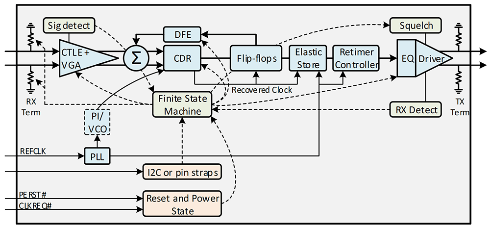
Figure 1: Retimer Block Diagram
Approach
A how-to guide is presented to help system engineers approach the PCIe 5.0 and CXL system design challenge in a methodical and bounded manner.
The proposed steps include:
- Determine if a Retimer is required. Use the statistical eye analysis simulator (SeaSim) tool to determine if the topology meets the PCIe channel requirements, if it is marginal to those requirements and may benefit from a Retimer, or if it clearly does not meet the requirements and cannot operate without a Retimer. Consider the performance degradations associated with temperature, humidity, and manufacturing variations.
- Define a simulation space. Identify the worst-case conditions (e.g. temperature, humidity, and impedance) and the minimum set of parameters (e.g. transmitter Presets) which must be varied to adequately analyze system performance and margin.
- Define the evaluation criteria. Determine the minimum eye height and width which will be considered a passing result and the minimum set/number of transmitter settings which must yield a passing result to have high confidence that there is adequate margin.
- Execute the simulation matrix and analyze the results. Use IBIS-AMI models and time domain simulations to analyze each case in the context of the pre-defined evaluation criteria.
The purpose of this analysis is to be more instructional than theoretical, leaving the reader with a concrete set of steps that can be applied whenever they are faced with a similar design challenge involving RC, Retimer, EP, and PCB material co-optimization.
Step 1: Determine if a Retimer is Required
Before evaluating an RC + Retimer + EP Link, you must first understand whether a Retimer is required for the Link. There are typically two ways of reaching this conclusion:
- Compare the end-to-end channel insertion loss, including RC and EP package losses, against the PCIe channel budget (Table 1). If the topology’s channel loss exceeds the PCIe informative specification, then a Retimer is likely required.
- Simulate the channel s-parameter in the Statistical Eye Analysis Simulator (SeaSim) tool which implements a reference PCIe transmitter and PCIe receiver to determine if the post-equalized eye height (EH) and eye width (EW) meet the minimum eye opening requirements for the reference receiver: ≥15 mV EH and ≥0.3 UI EW at Bit Error Ratio (BER) ≤ 10-12. If the eye opening does not meet the reference receiver’s requirements, then a Retimer is likely required. This methodology is more accurate and preferred to the pure loss budget analysis, as it takes into account other channel characteristics, such as reflections and crosstalk, as well as reference PCIe device equalization capabilities.
In this analysis we consider a two-connector PCIe topology which is common in server, storage, and accelerator systems (Figure 2).

Figure 2: System Board + Riser Card + AIC Topology
The topology includes various loss components for which PCIe has established a budget. Table 1 shows the breakdown of these loss components for PCIe 4.0 (reference) and PCIe 5.0 & CXL.
Table 1: Total Channel Insertion Loss Budget Breakdown

1. System Board budget includes the baseboard, riser card, the baseboard-to-riser-card, and PCIe card electromechanical (CEM) form factor connectors
Topology 1: No Retimer, Ultra-Low-Loss PCB Material
For such a topology, the main challenge at 32 GT/s is meeting the system board loss budget (16 dB at 16 GHz) for a 12-inch baseboard channel plus riser card. For the first topology analyzed in this paper, an ultra-low-loss PCB material such as Megtron-6 (~1 dB/inch at 16 GHz) is used for this topology to reduce the baseboard loss as much as possible, as shown in Figure 3.

Figure 3: Topology 1 using Ultra-Low-Loss PCB Material
Although such systems typically operate at nominal temperature (~25 C) and humidity (45-55%), it is important to examine the channel characteristics at extreme conditions such as high temperature (80 C), high humidity (>75%), and worst-case PCB trace manufacturing tolerance leading to differential pair impedance deviation (85 Ω + 10% = 93 Ω). Under these circumstances, the insertion loss degrades to ~1.11 dB/inch at 16 GHz. The channel s-parameters for this topology across different operating conditions are shown in Figure 4 below.
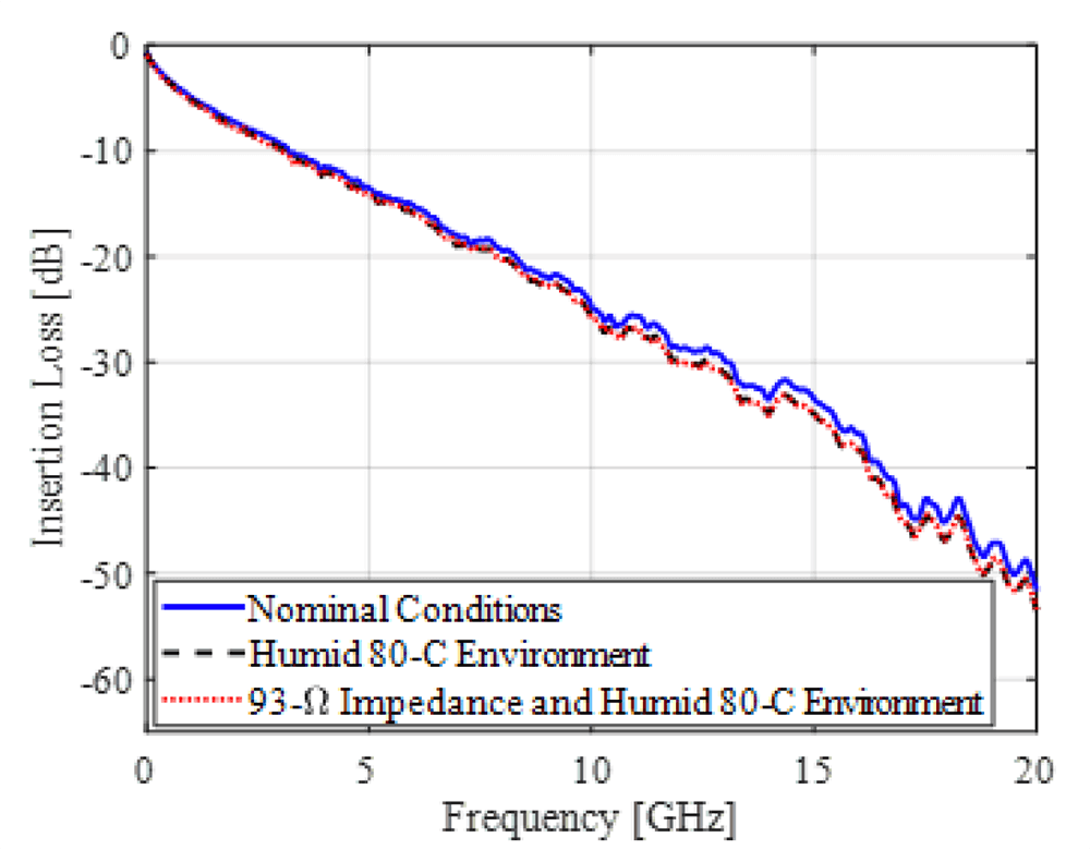
Figure 4: Topology 1 End-to-End Channel Insertion Loss for Nominal Conditions, Humid 80-C Environment , and 93-Ω Impedance and Humid 80-C Environment
To further confirm that a Retimer is required for this topology to operate, SeaSim simulations, shown in Figure 5, are run for each scenario: (a) nominal temperature/humidity conditions (differential pair impedance 85 Ohm, temperature ~25 C and humidity 45-55%), (b) high temperature/humidity (differential pair impedance 85 Ohm, temperature ~80 C and humidity 75%), and (c) 93-Ω impedance with high temperature/humidity (differential pair impedance 93 Ohm, temperature ~80 C and humidity 75%).
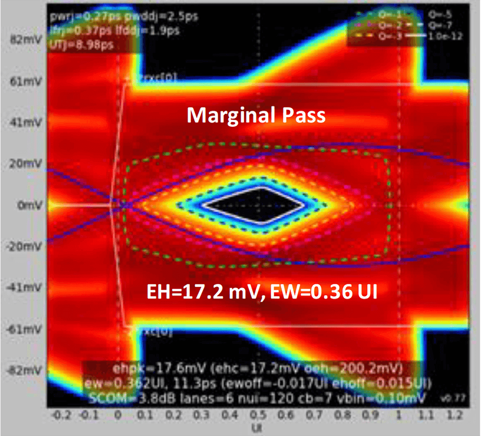
Figure 5a: SeaSim Result for Nominal Conditions
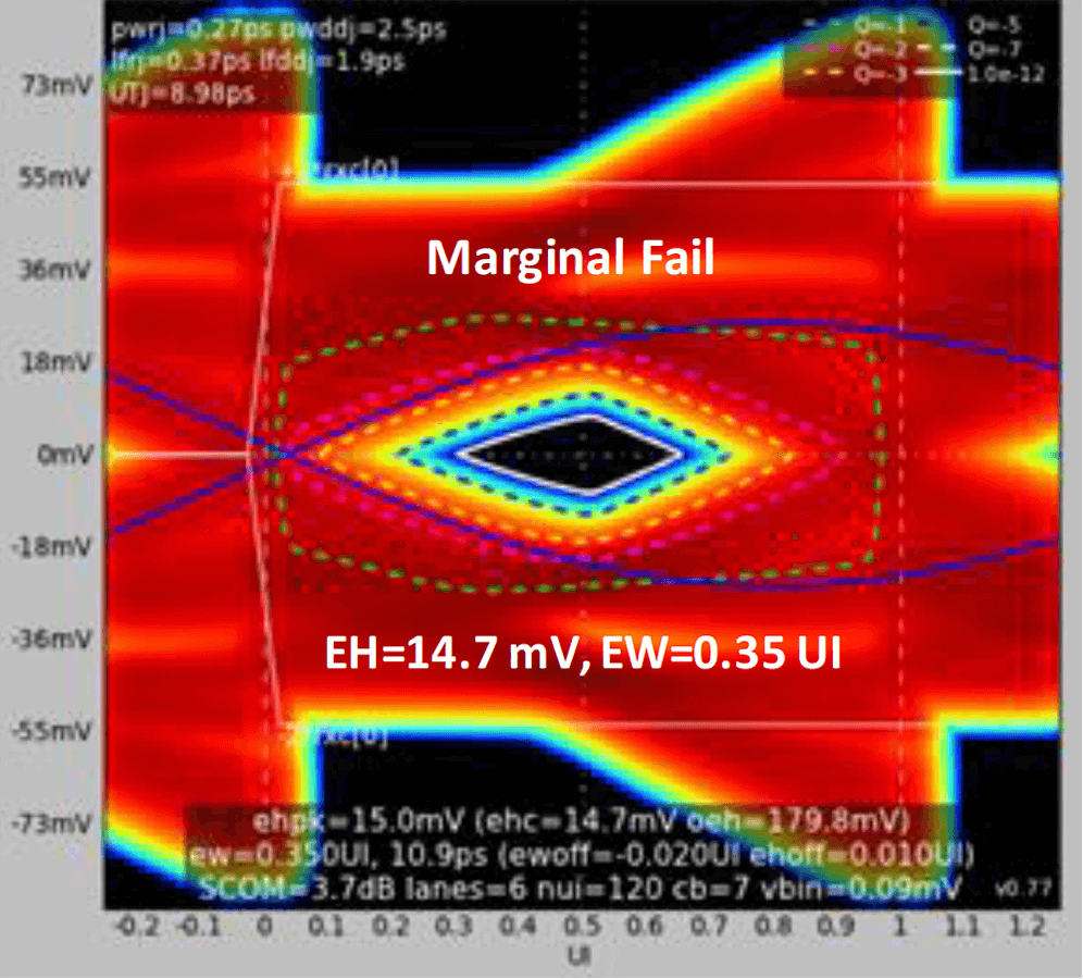
Figure 5b: SeaSim Result for Humid 80-C Environment
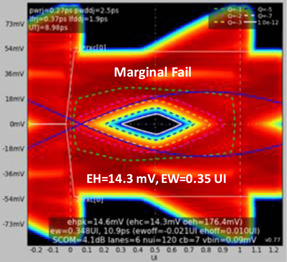
Figure 5c: SeaSim Result for 93-Ω Impedance and Humid 80-C Environment
IBIS-AMI channel simulations performed in bit-by-bit mode, which is analogous to time domain simulations, with a reference transmitter and reference receiver model also yields a post-equalized eye that does not meet the minimum eye dimensions of criterion 2. Figure 6 shows the testbench used for this simulation.

Figure 6: Keysight ADS Simulation Schematic for Topology 1
The transmitter IBIS-AMI model represents a reference transmitter with three-tap finite impulse response (FIR) filter as defined in the PCIe specification. Likewise, the receiver IBIS-AMI model represents a reference receiver with a four-pole/two-zero continuous time linear equalizer (CTLE) and a three-tap decision feedback equalizer (DFE) as defined in the PCIe specification.
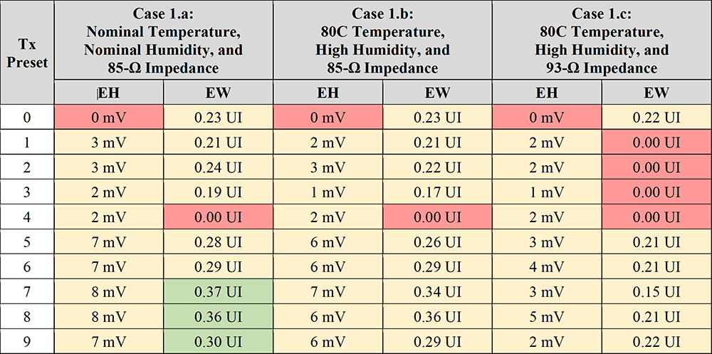
Three sets of IBIS-AMI simulations are performed to further validate the initial finding that a Retimer is needed for this channel topology (refer to Figure 4 for insertion loss plots). The simulation results are summarized in Table 2.
1.a) Topology 1 assuming nominal temperature, nominal humidity, and 85-Ω impedance
1.b) Topology 1 assuming high temperature (80 C), high humidity, and 85-Ω impedance
1.c) Topology 1 assuming high temperature (80 C), high humidity, and 93-Ω impedance
Table 2: Results Summary for Topology 1
(Reference Receiver with 15-dB CTLE gain and adaptive CDR/DFE)
Topology 2: Retimer on Riser Card, Ultra-Low-Loss PCB Material
Given that the channel in Topology 1 fails both channel evaluation criteria, a second topology is considered in which a Retimer is added on the Riser Card, as shown in Figure 7. Adding a Retimer segments the channel into two independent halves, making it much easier to meet the PCIe channel specifications on each half.

Figure 7: Topology 2 with Retimer on Riser Card using Ultra-Low-Loss PCB Material
Taking into account additional Retimer breakout routing and considering the worst-case conditions—high temperature, high humidity, and 93-Ω impedance due to manufacturing tolerance—the insertion loss for the two channel segments in Topology 2 are shown in Figure 8.
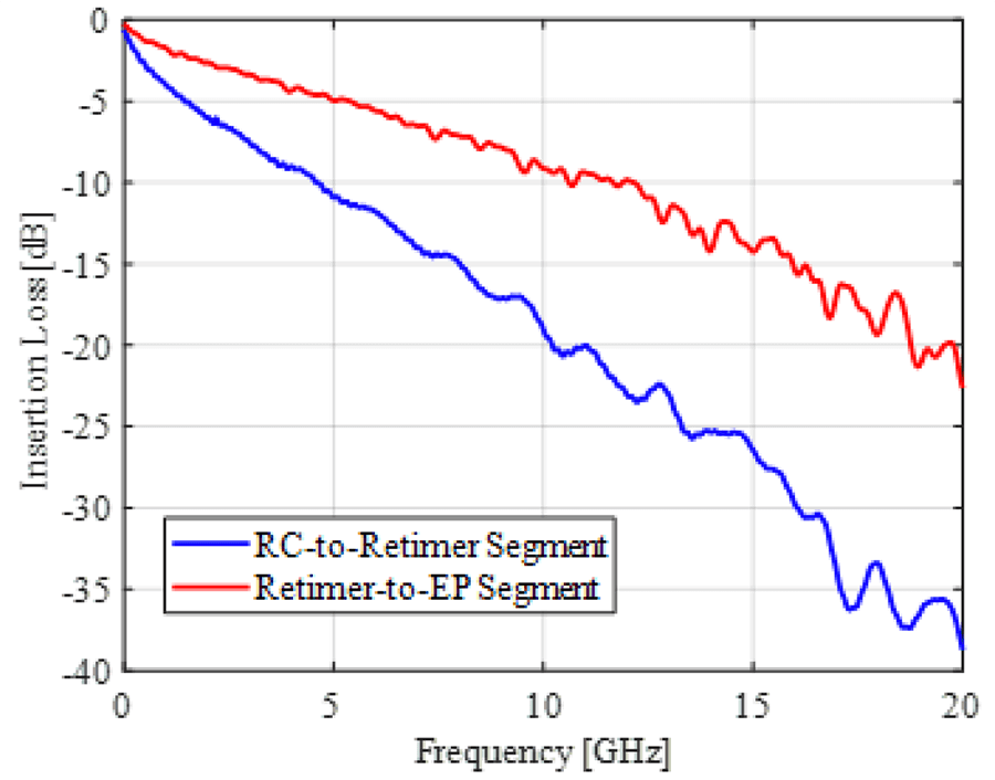
Figure 8: Topology 2 End-to-End Channel Insertion Loss for RC-to-Retimer Segment and Retimer-to-EP Segment
With considerably lower insertion loss, the SeaSim analysis shows there is ample margin for both Link segments, as shown in Figure 9.
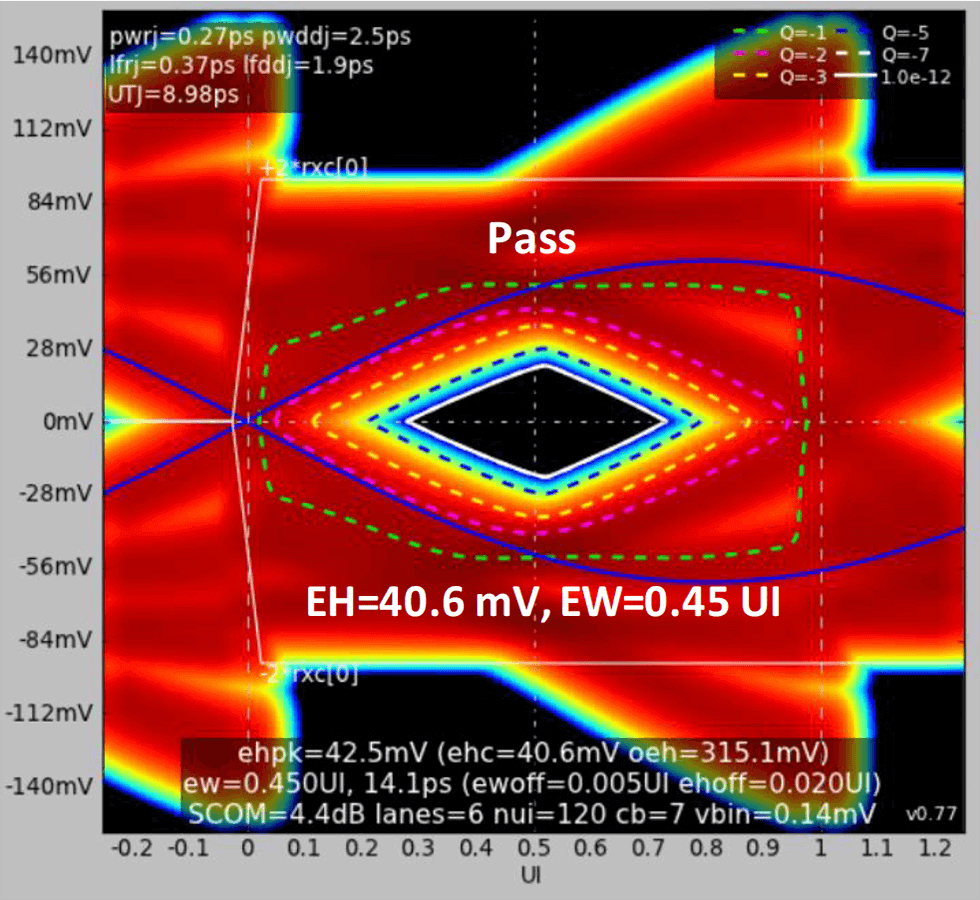
Figure 9a: SeaSim Result for RC-to-Retimer Segment
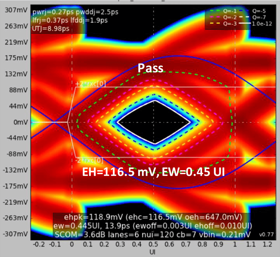
Figure 9b: SeaSim Result for Retimer-to-EP Segment
Topology 3: Retimer on Baseboard, Low-Cost PCB Material
Space permitting, instead of the Riser Card, a Retimer can also be placed on the Baseboard as it is shown in Figure 10. With such a Retimer placement, the margins for each channel segment are relatively large compared to the “without Retimer” case. At this point, system designers can consider using higher loss PCB material to reduce the cost of the system. A lower cost material such as Megtron-4 will have ~1.9 dB/inch at 16 GHz under worst-case conditions and result in a 40-50% cost reduction in the baseboard.

Figure 10: Topology 3 with Retimer on Baseboard using Low-Loss PCB Material
Considering the worst-case conditions, the insertion loss for the two channel segments in Topology 3 are shown in Figure 11.
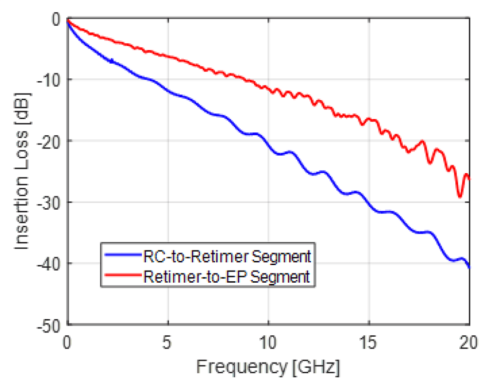
Figure 11: Topology 3 End-to-End Channel Insertion Loss for RC-to-Retimer Segment and Retimer-to-EP Segment
Despite higher loss per inch on the baseboard with the lower cost PCB material, there is still a considerable margin for both Link segments, as shown in Figure 12.
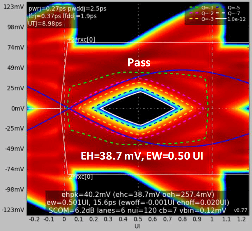
Figure 12a: SeaSim Result for RC-to-Retimer Segment
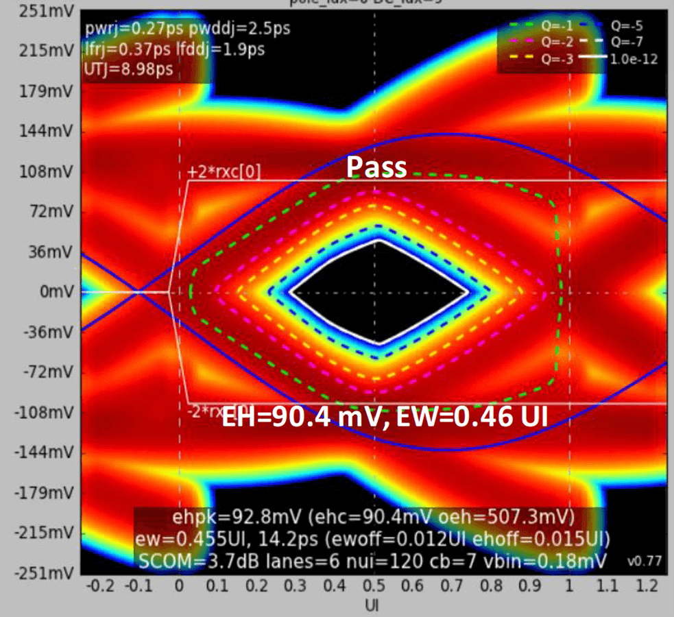
Figure 12b: SeaSim Result for Retimer-to-EP Segment
Step 2: Define a Simulation Space
The high-level simulation parameters used in all IBIS-AMI simulations presented in this work are shown in Table 3.
Table 3: Summary of High-Level Simulation Parameters

To achieve meaningful results in a reasonable timeframe, a narrow simulation space is chosen, as shown in Table 4. The approach used for selecting the simulation space is covered in a prior work [3], and the basic idea is to test multiple transmitter Preset settings as a means of gauging how robust the Link performance is. If a channel can pass for multiple Preset settings, this is a good indicator of healthy margin compared to a case where only one Preset works.
Table 4: Simulation Space

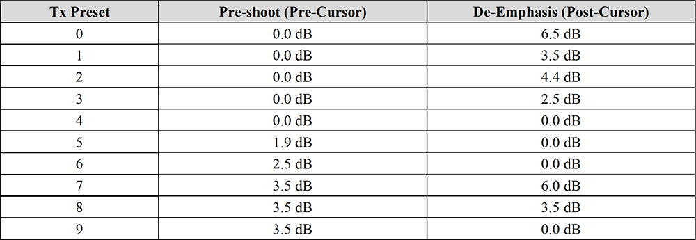
Transmitter Presets are pre-defined combinations of pre-shoot (pre-cursor equalization) and de-emphasis (post-cursor equalization). Table 5 shows the list of Preset settings considered in this analysis. It is worth noting that the every PCIe transmitter may implement slightly different pre-shoot and de-emphasis values for the ten defined presets, however the PCIe standard does define tolerances for these values with which every PCIe transmitter must comply.
Table 5: Transmitter Preset Settings
Keysight Advanced Design System (ADS) is the tool used to execute the IBIS-AMI simulations, measure the extrapolated EH and EW, and plot the post-equalized eye opening. For Topologies 2 and 3, two separate testbenches—RC to Retimer and Retimer to EP—are used to simulate the two separate Link segments, as shown in Figure 13 and Figure 14 below.
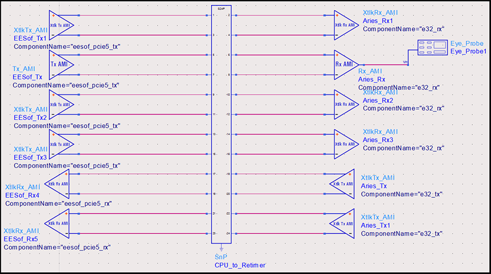
Figure 13: Keysight ADS Simulation Schematic for Topologies 2 and 3, RC to Retimer
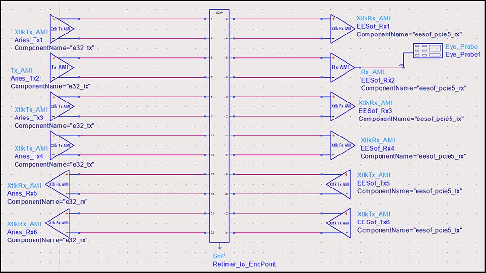
Figure 14: Keysight ADS Simulation Schematic for Topologies 2 and 3, Retimer to EP
Step 3: Define the Evaluation Criteria
This analysis uses similar pass/fail criteria to that which was used in a prior work [3]. The criteria consist of two rules:
- A link must meet the receiver’s eye height (EH) and eye width (EW) requirements
- A link must meet criterion 1 for at least half of Tx Preset settings (≥5 out of 10)
Criterion 1 establishes that the there is a viable set of settings which will result in the desired BER. The specific EH and EW required by the receiver is implementation-dependent. For example, the Astera Labs receiver model requirements for post-equalized EH and EW are shown in Table 6. Criterion 2 ensures that the link has adequate margin and is not overly-sensitive to the Tx Preset setting.
Table 6: Astera Labs Receiver Model EH and EW Requirements

Step 4: Execute the Simulation Matrix and Analyze the Results
Topology 2 is simulated using the parameters and Tx Preset values noted in Step 2. Note that the minimum eye height and eye width requirement is set by the receiver model. For the Astera Labs Receiver model, the requirements are listed in Table 6. For the reference receiver model, the requirements are set by the PCIe standard.
Table 7: Topology 2 Results
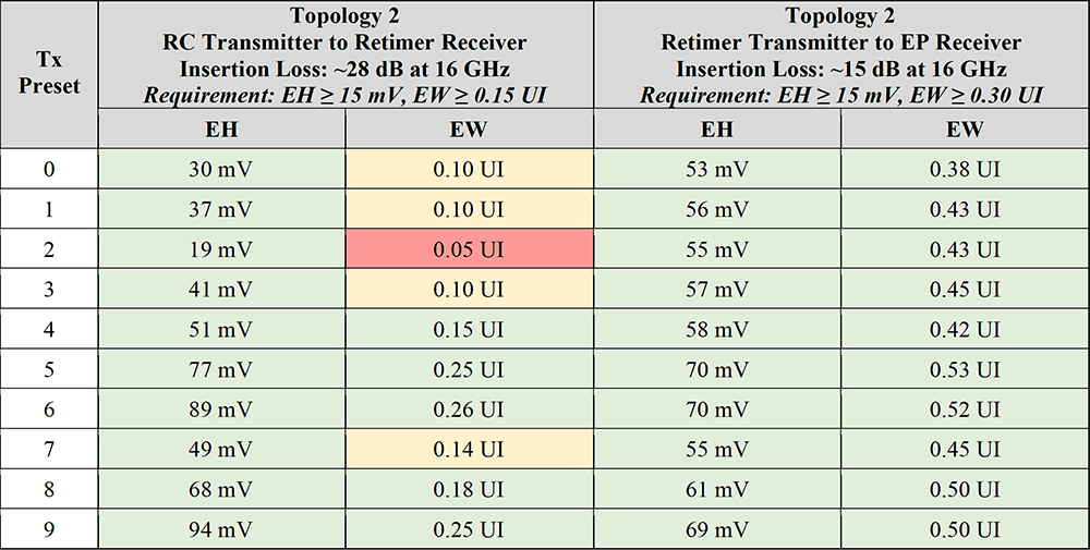
Table 8: Topology 3 Results
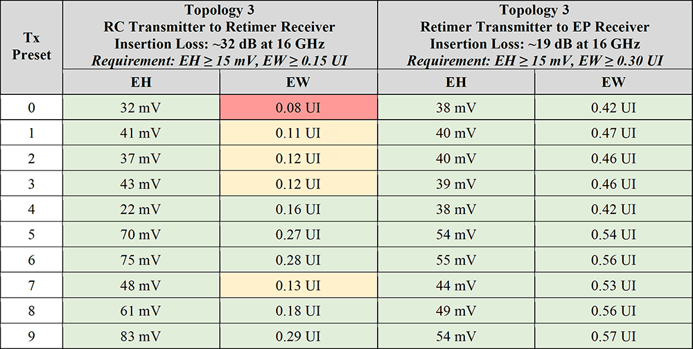
A detailed data display of the pre-equalized channel pulse response and post-equalized eye contour are shown in Figure 15 and Figure 16 for Topology 2 and Topology 3, respectively.
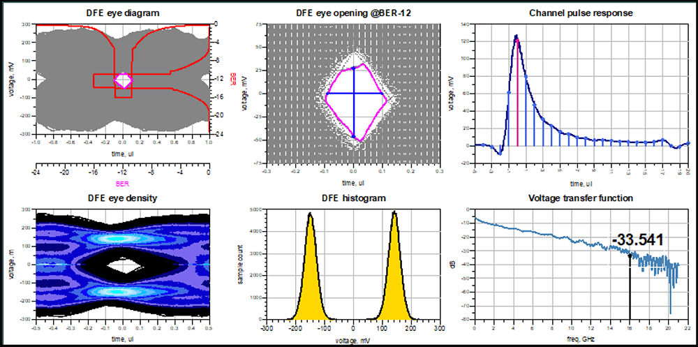
Figure 15: Detailed Data Display for Topology 2, Tx Preset 9
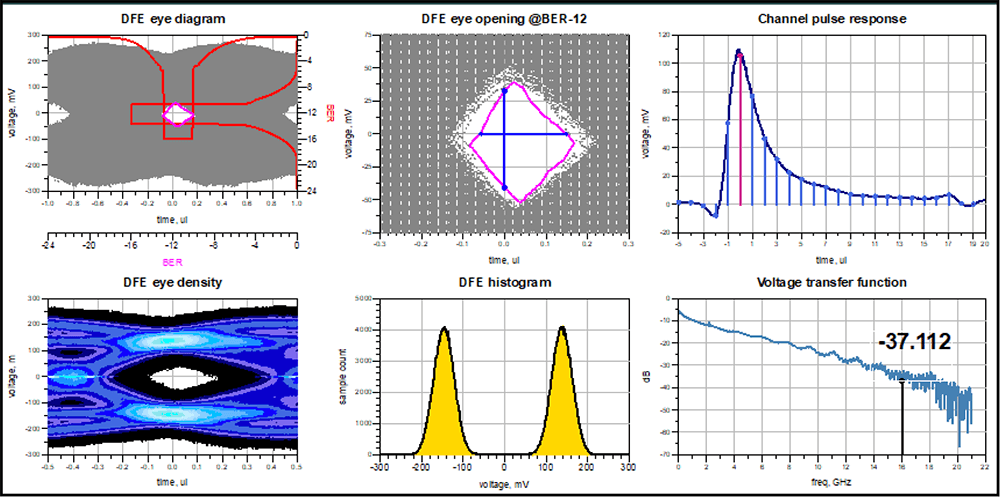
Figure 16: Detailed Data Display for Topology 3, Tx Preset 9
Conclusions
This analysis shows that a channel topology which is common to PCIe 5.0 and CXL-based, at 32GT/s, server designs—baseboard plus riser card plus add-in card—may exceed the PCIe channel specifications and also the capabilities of a generic transmitter/receiver pair. By segmenting this channel topology into two with the use of a protocol-aware Retimer, simulations demonstrate that a more rigorous pass/fail criterion—achieving adequate eye height and width across at least half of all transmitter preset settings—can be met.
In fact, this analysis shows there is enough margin to allow for less expensive PCB material to be used, potentially reducing the total cost of the system substantially while still achieving robust performance on both link segments. This methodology of (1) determining if a Retimer is required, (2) defining a simulation space, (3) defining the evaluation criteria, and (4) executing the simulation matrix can be applied to a wide varied of PCIe 5.0 and CXL applications to help assess system performance and cost tradeoffs.
References
[1] https://pcisig.com/
[2] https://www.computeexpresslink.org/
[3] Yongyao Li, et al, “End-to-End System-Level Simulations with Repeaters for PCIe Gen4: A How-To Guide”, DesignCon 2017
Author Biographies
Elene Chobanyan is a signal integrity engineer at Hybrid IT Compute Solutions at Hewlett Packard Enterprise (HPE). She is HPE's primary voting member at PCI-SIG Electrical workgroup, a representative at IPC D24D standard and an active contributor at Gen-Z PHY workgroup. Elene received the B.S. degree in physics and the M.S. degree in electrical and electronics engineering from Tbilisi State University, Tbilisi, Georgia, and PhD. Degree in electrical and computer engineering from Colorado State University, USA. Her current focus areas are high speed server interconnect architecture and design, PCB material characterization techniques, non-volatile and volatile memory subsystems.
Casey Morrison is the head of Product and Applications Engineering at Astera Labs and is responsible for defining, validating, and helping customers design-in Astera Labs’ semiconductor products and plug-and-play systems. With 12+ years of experience in high-speed interfaces for data center and wired/wireless communications systems, he has a passion for creating chips and systems which help to enable state-of-the-art compute and networking topologies.
Pegah Alavi is a Senior Applications Engineer at Keysight Technologies, where she focuses on Signal Integrity and High Speed Digital Systems and Applications. Prior to joining Keysight Technologies, Pegah worked on system level modeling of analog and mixed signal circuits in order to best predict the overall systems performance and accurately represent each component.


