
The Impact of Bit Errors in PCI Express® Links: The Painful Realities of Low-Probability Events
Peripheral Component Interconnect Express (PCIe®) 5.0 ushers in the era of >1 terabits per second (Tbps) of data bandwidth. Such immense bandwidth would be typical of a 16-lane (x16) link between two PCIe nodes, each lane operating at 32 Gbps.
Given that the PCIe base specification mandates that a bit error ratio (BER) on each transceiver lane must be 1E-12 or better – that is, less than one error every 1E12, or 1 terabit – a bit-flip error could happen within the link every 1 s! Even a PCIe 4.0 link, if designed for the same BER specification, would have a bit-flip error every 2 s.
Such bit errors are classified under the “correctable errors” category according to the PCIe specification. They do affect performance vis-à-vis latency and bandwidth, but no data/information is lost, and the PCIe fabric remains reliable. To get a better sense of the impact of errors, you need to consider the location of an error in the data stream and the time at which the error occurs in terms of the state of the PCIe Link Training and Status State Machine (LTSSM).
In the L0 LTSSM state where data packets are transmitted and received, an erroneous bit received within Data Link Layer Packets (DLLPs) would lead to a failure in the data integrity check performed using the cyclic redundancy check (CRC) included with each transmitted packet. One of the salient features of PCIe is to ensure robust transmission. When the Data Link Layer detects an errored packet, it sends a negative acknowledgement (NACK) to its link partner. Upon receiving the NACK, the link partner restarts transmission from that packet onward. If the BER is within the specification, the only cost is a small hit to the link throughput and a momentary impact on latency (which can be shown to be greater than three times the normal latency with some basic math).
Let’s now consider a more unforgiving example. PCIe uses a 128b/130b encoding scheme for 8.0-Gbps and higher rates. In this encoding scheme, each 130-bit block consists of a 2-bit sync header and a 128-bit data payload. There are two valid sync header encodings: 10b for data blocks and 01b for ordered set (non-data) blocks. Since these sync header bits occur every two bits within 130 bits, a simple probability analysis would reveal that, assuming all lanes are operating around the worst-case 1E-12 BER, there is a chance of an error happening on the sync header on some lane within a x16 link approximately once every minute.
Having received an invalid sync header in the L0 link state, the PCIe controller, per the PCIe base specification, is expected to suspend data traffic and take the link to the Recovery LTSSM state. Upon entering the Recovery state, the PCIe controller allows the physical layer (PHY) transceivers to retrain, reacquire block lock and so on, thus getting an opportunity to re-establish optimal link health. The specification allows up to 1 µs for a trip through the Recovery LTSSM state. Needless to say, this adds a huge delay to the original errored packet – and all subsequent packets – until the link goes back to the L0 state.
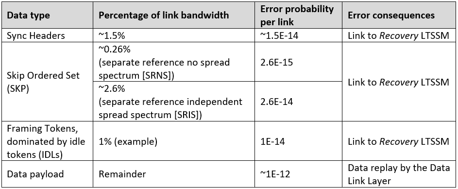
Besides sync headers, there are other protocol-related overhead tokens and data sets which, if corrupted, can also lead the link into the Recovery state. Table 1 shows the approximate probabilities of various data types being in error and the consequences of those errors.
At this point, it’s worth noting that PCIe 5.0 introduces selectable “precoding,” which breaks an error burst into two errors: an entry error and an exit error. While this helps manage a burst of errors (caused by error propagation in a PHY receiver), it basically comes at a cost of turning a random single-bit error into two errors, thereby doubling the net BER and the aforementioned error probabilities.
Tallying up all of the above, it is conceivable that a x16 PCIe 5.0 link would enter the Recovery LTSSM state approximately every 10 s, and it would replay a transaction layer packet (TLP) approximately every 1 s.
Such frequent unplanned entries to the Recovery state (every 10 s) and TLP replays (every 1 s) will cause system health monitors in the baseboard management controller (BMC) to raise an alarm, and contribute to “latency tails,” which can have a considerable performance impact at the application layer [1].
So what can you do to extract the full potential of a PCIe 5.0 link and avoid annoying, hard-to-diagnose “glitches” in the higher application layers? Well, one of the obvious solutions would be to design a system board with lower transmission (or insertion) loss in the channel. Using the SeaSim simulation tool from the PCI Special Interest Group (SIG) [2], Figure 1 shows eye diagrams from two channels: one with 31 dB of insertion loss and another with a higher 33-dB insertion loss. The simulations have two different BER targets: 1E-12, according to the specification; and 1E-21, which is akin to saying no errors at all. To ensure these BERs, the simulated eye height must meet or exceed 15 mV.
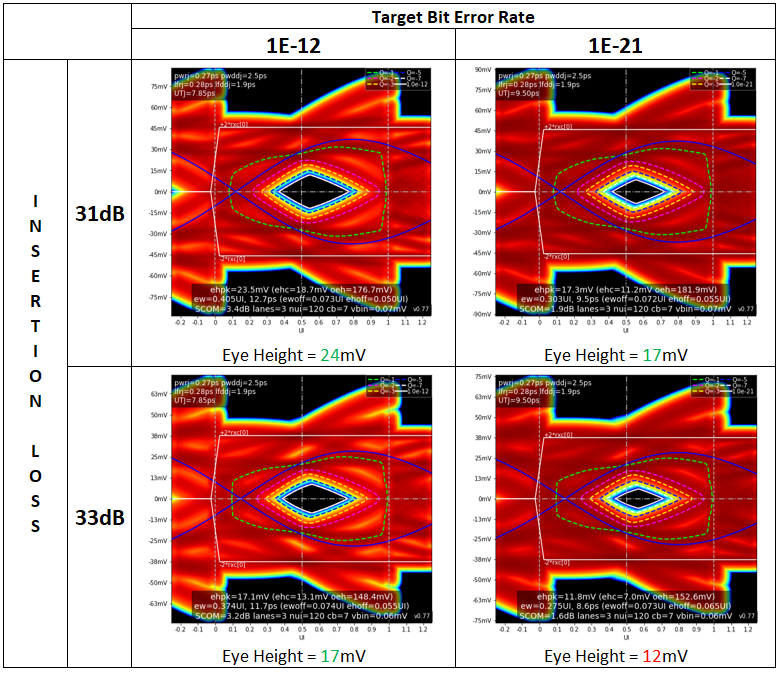
You can see from these simulations that while the 33-dB loss channel would “pass” for a bit error target of 1E-12, it would not pass at 1E-21. The 31-dB loss channel does pass at 1E-21, however, with an eye height equivalent to the 33-dB channel at 1E-12. So in this very distinct analysis, backing off the insertion loss by 2 dB or so would imply going from the link entering the Recovery state every 10 s to almost never doing so at all.
Upgrading printed circuit board (PCB) material to reduce transmission loss is a viable option to gain 2 dB of insertion loss, but may add a considerable expense, depending on board size. Alternatively, enhancements to PHY-layer transceiver circuitry to boost performance come at the cost of silicon power, area and complexity. And then there are certain system topologies that may turn out be marginal even when combining best-in-class transceiver technology and PCB materials, so aiming to achieve lower BERs on these topologies may be next to impossible. In such scenarios, you could take a divide-and-conquer approach by employing a PHY protocol-aware extension device, referred to in the PCIe specifications as a retimer. A retimer would split a stringent channel into separate smaller electrical link segments, each of which can operate with enough margin to achieve drastically lower BERs.
While fairly limited at PCIe 3.0, such considerations became more widespread with current PCIe 4.0 deployments and will only grow with PCIe 5.0, as the signal integrity challenges far outpace the doubling of data rates.
PCIe 5.0 systems are likely to see noticeably greater occurrences of link errors and TLP retries than current-generation systems. Thus, you must take care when setting a BER target for a PCIe link within a system. System designers typically account for device and environmental variations and set aside some electrical performance margin to safely keep a link operating at a BER mandated by the base specification. You must also factor in application-layer considerations given the nature of future data-center workloads, however. It would be prudent to target lower BERs for PCIe 5.0 and beyond.
Citations
1. Deierling, Kevin. “In Modern Datacenters, The Latency Tail Wags The Network Dog.” Nextplatform.com, March 27, 2018.
2. PCI SIG Seasim Software Package